


| Name | 16-point DC Input/16-point Transistor Output Unit witd MIL Connectors (Sinking Outputs) | ||
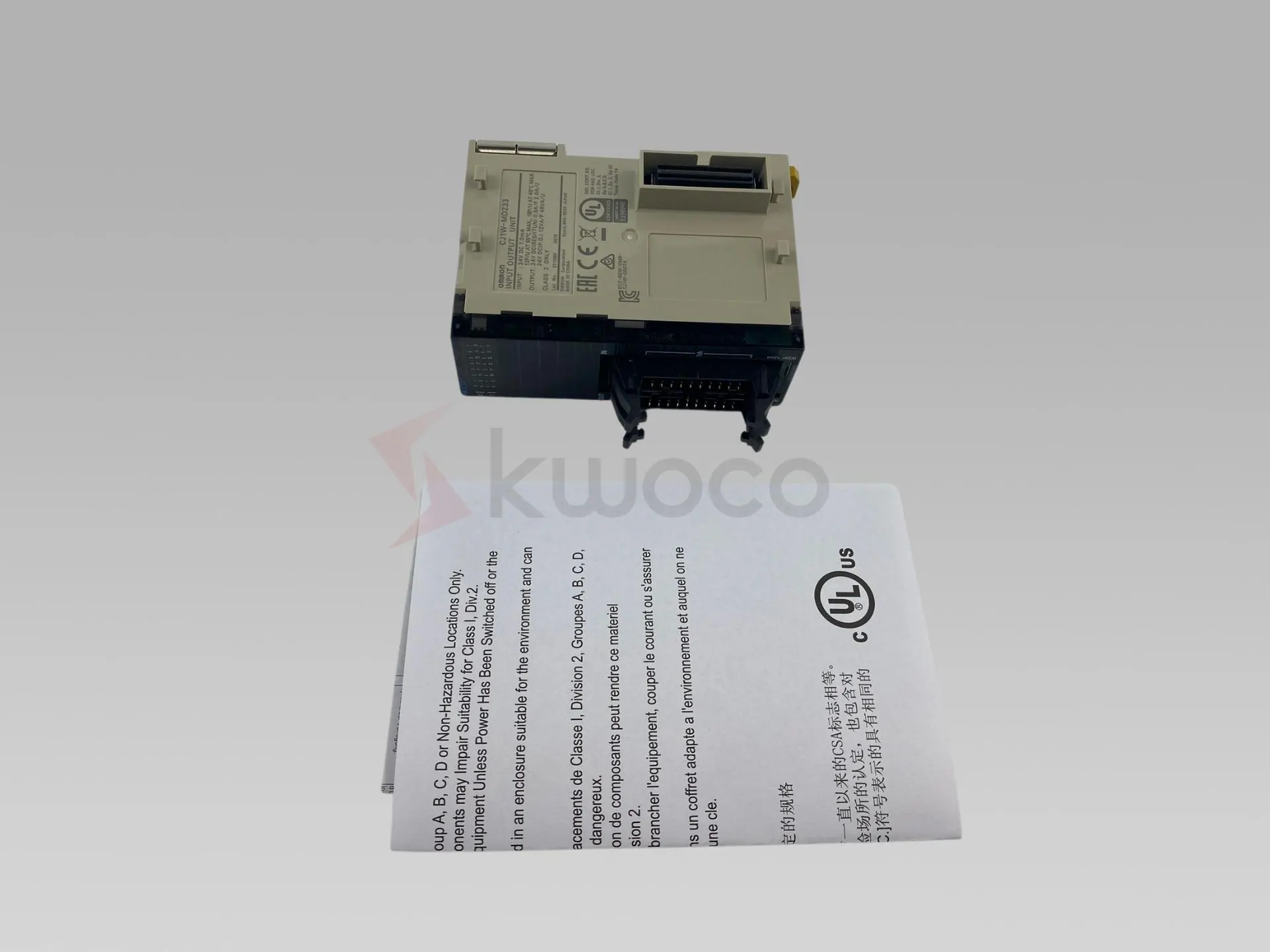
| Model | CJ1W-MD233 | ||
| Output section (CN1) | Input section (CN2) | ||
| Rated Voltage | 12 to 24 VDC | Rated Input Voltage | 24 VDC |
| Operating Load Voltage Range | 10.2 to 26.4 VDC | Operating Input Voltage | 20.4 to 26.4 VDC |
| Maximum Load Current | 0.5 A/point, 2.0 A/Unit | Input Impedance | 3.3 kΩ |
| Maximum Inrush Current | 4.0 A/point, 10 ms max. | Input Current | 7 mA typical (at 24 VDC) |
| Leakage Current | 0.1 mA max. | ON Voltage/ON Current | 14.4 VDC min./3 mA min. |
| Residual Voltage | 1.5 V max. | OFF Voltage/OFF Current | 5 VDC max./1 mA max. |
| ON Response Time | 0.1 ms max. | ON Response Time | 8.0 ms max. (Can be set to between 0 and 32 in tde Setup.) * |
| OFF Response Time | 0.8 ms max. | ||
| No. of Circuits | 16 (16 points/common, 1 circuit) | OFF Response Time | 8.0 ms max. (Can be set to between 0 and 32 in tde Setup.) * |
| Fuse | None | ||
| External Power Supply | 10.2 to 26.4 VDC, 20 mA min. | No. of Circuits | 16 (16 points/common, 1 circuit) |
| Number of Simultaneously ON Points | 75% (at 24 VDC) | ||
| Insulation Resistance | 20 MΩ min. between tde external terminals and tde GR terminal (at 100 VDC) | ||
| Dielectric Strengtd | 1,000 VAC between tde external terminals and tde GR terminal for 1 minute at a leakage current of 10 mA max. | ||
| Internal Current Consumption | 5 VDC 130 mA max. | ||
| Weight | 90 g max. | ||
| Accessories | None | ||
| Circuit Configuration | CN1 (OUT) | CN2 (IN) | |
 |   | ||
| External connection and terminal-device variable diagram | CN1 (OUT) | CN2 (IN) | |
 |  | ||


